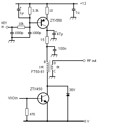
Keying and Driver Stages
The keying stage consists of a ZTX550 transistor which switches the collector supply of the driver stage. The components in the base and collector of the ZTX550 are chosen to give a rise and fall time of the keyed rf of around 4ms and reduce keyclicks - on air use indicates these values are ideal.
The ZTX450 driver produces sufficient output for the pa transistor. Its output is coupled by a toroidal transformer wound on a T50-61 ferrite ring.
The keying and driver stages are also powered at all times. For netting purposes operation of the key produces a low level signal which can be tuned to the listening frequency.
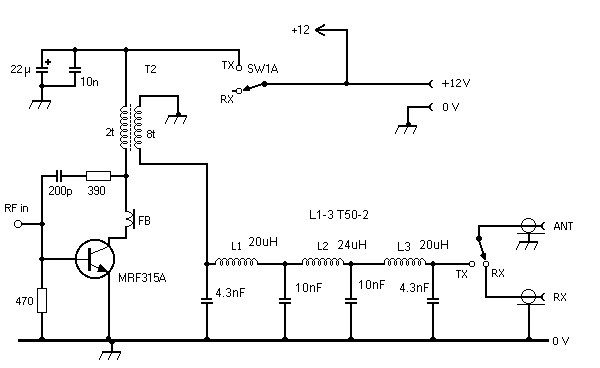
PA and Low Pass Filter
The PA uses a Motorola MRF315A 144MHz turnstile transistor - no particular reason for this choice, except that I had a few in the junk box and I had also used it in the 5MHz transmitter. It is configured as a conventional class C stage. The output transformer T2 is wound on a 26mm diameter 3C85 core.
The low pass filter is from a design by David G0MRF designed to give good rejection of the second harmonic (which is in the broadcast MW band). I used T50-2 toroids rather than the larger T130-2 ones David used. These are adequate for 10W but the wire is fairly tight as more turns are needed. Do NOT use T50-61 toroids, they get VERY warm!
A ferrite bead is required on the collector connection - a single wire through the bead. Without it the PA is unstable, as being a VHF transistor it has considerable power gain at these frequencies.
The Transmit/Receive switch SW1 connects the 12V to the PA on transmit. A second pole is used for switching the antenna. The PA produces around 6W from a 12V supply.
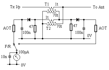
A simple SWR meter circuit is connected in the transmitter output and is useful as an antenna tuning aid and rf current meter. The value of the AOT resistors depends on the sensitivity of the meter, and 680 ohms was found suitable at G3YMC - adjust for full scale deflection in the forward direction. T1 and T2 are wound on the same T50-61 torroids as used in the transmitter. The diodes should be point contact or germanium ones with low forward voltage drop (eg OA91).
Construction
The transmitter is built in a suitable diecast box. A PL259 connector is used for the antenna, phono sockets for the keyer and receiver connections, and a double pole toggle switch for the receive/transmit switching. Current consumption is around one amp and any convenient 12V power supply can be used.